Introduction: Welcome to the "Mass Production Plan" of China exportsemi net, here we will show you the latest and hottest mass production plans of Chinese local manufacturers. If you are interested in this, feel free to contact us for more information (china.exportsemi@ehaitech.com).
Modern power electronics applications are based on the switching technology of power semiconductor devices, and these power switching devices need an effective gate drive scheme in operation. Gate driver is the key component to connect power devices and microcontrollers. By receiving the control signals sent by microcontrollers (MCU/DSP), it provides the gate driving voltage required by power switching devices, and realizes the opening and closing of power devices, thus meeting the needs of various power electronic applications.
Company A's latest grid driver solution (mass production solution 12) focuses on the application of household appliances, industrial new energy and other fields, providing customers with high reliability and low cost grid driver solutions.

Figure 1: Applications for Household Appliances
Characteristics of the product
Production Scheme 12 has 650V switch node withstand voltage, 300mA and 1000mA output peak pull current and fill current capability, and is specially designed to drive power MOSFETs or IGBTs. In the case of switch node VS transient-60V (100ns), it can ensure the normal operation of the system and can cope with the demand of dv/dt variation as high as 100V/ns.
In addition, the mass production plan 12 has built-in a number of perfect protection functions, including: when the input floats or the input pulse width is insufficient, the output will remain low; It has built-in interlocking and dead zone protection functions to effectively prevent the high and low side drives from opening at the same time; At the same time, high-side and low-side UVLO protection makes the system more reliable.
For household appliances, industrial new energy and other applications, reliability is the primary consideration for customer device selection. For gate drivers, reliability can be measured from the following aspects.
Highlight 1: Negative pressure capability of switch nodes
In half-bridge topology applications, inductive loads are usually used. At the same time, because of the parasitic inductance of power devices and power circuits, when the high-side power transistor is turned off, the freewheeling circuit will generate negative pressure at the switching node. The negative pressure consists of a parasitic inductor L3, L4Resulting in a large dynamic peak negative pressure and a parasitic resistance from the line and the lower tube body diode D2The lower static negative pressure caused by conduction is shown in Figure 2.

Figure 2: Switched Current Path and VS Voltage
When the negative pressure of the switch node is larger, the internal devices of the gate drive chip bear higher voltage stress, which makes it easier to break down and fail. At the same time, the higher the negative voltage of switch node VS, the lower the transient voltage of HB at the high-side power supply node of gate driver chip. When the HB voltage is lower than the reference ground COM, the internal parasitic diode conduction may cause logic error or chip burning, which may affect the reliable operation of gate driver. Therefore, higher negative pressure bearing capacity of switch nodes can improve the reliability of power system under severe working conditions.
According to the measured data, under the same test conditions, several similar products on the market are comprehensively compared and tested, and the negative pressure bearing capacity of mass production scheme 12 is equivalent to that of international first-line brands, which is at the domestic advanced level.

Table 1: Comparison of negative pressure capacity between mass production scheme 12 and several similar products in the market
Highlight 2: High dv/dt noise suppression capability of switching nodes
The high-side driving circuit of high-voltage half-bridge gate driver mostly adopts bootstrap circuit structure, and the low-voltage logic control signal can be transmitted to the high-side by using the level shift circuit inside the gate driver. Because the high-side control drive circuit refers to the switching node VS, the parasitic current in the chip will be transmitted to the low-voltage side through the coupling path in the high-speed switching state. When there is mismatch in the chip, differential mode interference signals will be generated, thus affecting the correct input and output logic.
Mass production scheme 12 adopts the unique level shift and common-mode noise suppression technology of Company A, which can effectively suppress the common-mode noise interference generated during the high-speed switching of switch nodes and prevent false triggering, thus ensuring the normal and reliable operation of the system.
Highlight 3: Lower propagation delay and delay matching
In half-bridge switching circuits, propagation delay and delay matching are the key parameters of gate drivers. Lower propagation delay means faster response capability, such as short-circuit protection or accurate current limiting, which requires short response time of control loop.
In addition, the propagation delay between the high side and the low side of the gate driver may also be different. Due to the differences between the internal circuits and devices of the chip (for example, the propagation delay of the high side driver is longer than that of the low side driver), the high-level drive signals output by the high and low sides may overlap in some switching periods (even including dead time). If this happens, a short circuit will occur and the power switching device or load will be damaged. Comprehensive comparison and test of several similar products on the market show that mass production scheme 12 has lower propagation delay and delay matching.

Table 2: Comparison of propagation delay and delay matching between mass production scheme 12 and competing products
Highlight 4: High driving current capability
There is crosstalk problem in practical application of half-bridge switching circuit. For example, when the high-side switching device is turned on while the low-side switching device remains turned off, the switching node VS voltage will rapidly rise to the bus voltage VBUS. During this process, the voltage across the Miller capacitor of the low-side switching device changes rapidly, resulting in displacement current Igd. This current causes a voltage drop through the gate turn-off resistance and the equivalent pull-down resistance inside the LO. If this voltage drop is greater than the turn-on threshold of the low-side switching device, the low-side device will be turned on, which may lead to the straight-through or damage of the half-bridge circuit. The mass production scheme 12 has a driving current filling capacity of 1000mA, which has a stronger displacement current absorption capacity and effectively solves this problem.
In practical applications, engineers usually need to trade-off between switching loss and EMI performance. Within the allowable switching loss range, appropriate driving resistors are usually connected in series between the output of the gate driver and the gate of the switching device to limit the turn-on speed of the switching device and thus optimize EMI performance. In different power segments, the optimized driving current requirements will be different. A larger driving current means that it can adapt to a wider range of power applications. Compared with several similar products in the market, the mass production scheme 12 products have higher peak driving current capability, providing engineers with more flexible and efficient solutions.

Figure 3: Crosstalk problem in half-bridge circuit
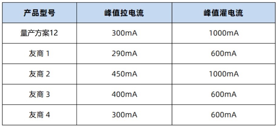
Table 3: Peak Drive Current Comparison of Production Scheme 12
Highlight 5: Other reliability performance
Production Scenario 12 not only integrates high and low side undervoltage locking (UVLO) function, but also ensures that the half-bridge gate driver can provide enough gate voltage for peripheral power devices to fully turn on the power devices. In addition, the mass production scheme 12 also has built-in interlocking and dead time protection functions, which can automatically insert the dead time when the output state changes, ensuring that the other side of the gate driver is completely closed before one side is opened, effectively preventing the common situation between the high and low sides.
In addition, the production scheme 12 also has the input pulse filtering function. In practical applications, switching operation of power devices may result in large dv/dt and di/dt, resulting in switching noise coupled to the control signal line connected to the gate driver. In this case, the input of the gate driver may be disturbed by the voltage spike, which leads to the wrong driving signal, thus making the switching device turn on or turn off by mistake, and then affecting the normal operation of the system. The input pulse filter integrated in the production scheme 12 can effectively filter out these peak noise signals and ensure the reliable operation of the system.
Comprehensive comparison and test of several similar products on the market show that mass production scheme 12 has high reliability, high costs performance and excellent performance index. It can meet the application requirements of most air ducts, ceiling fans, smoke machines, inverter power supplies, uninterruptible power supplies, etc.
If you are interested or have questions about this program, feel free to contact us and explain your appeal: china.exportsemi@ehaitech.com
You can also contact us directly by scanning: